


 Home
Home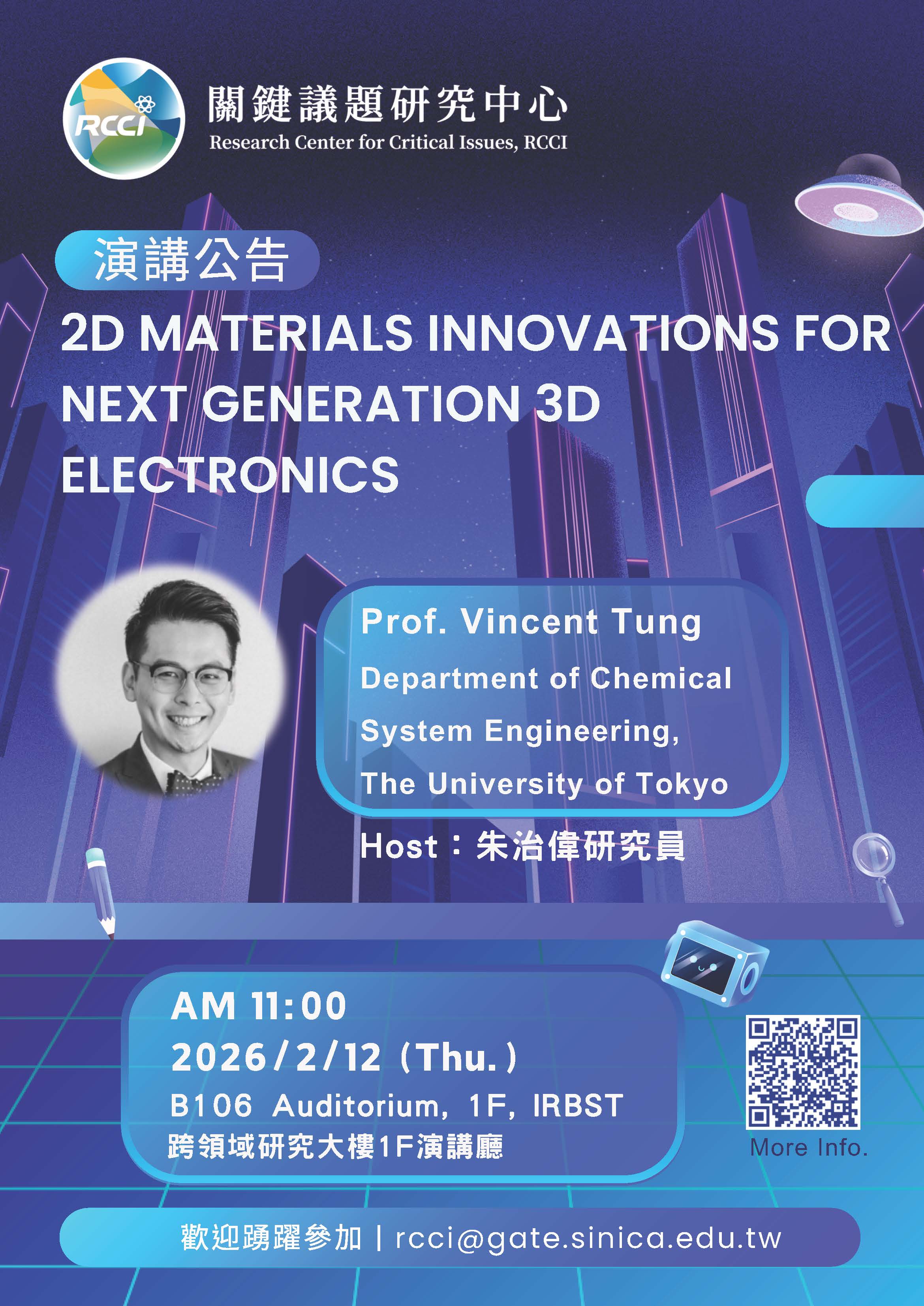
- Lectures
- Research Center for Critical Issues
- Location
B106 Auditorium, 1F, Interdisciplinary Research Building for Science and Technology, Academia Sinica
- Speaker Name
Prof. Vincent Tung (The University of Tokyo, Japan)
- State
Definitive
- Url
2026-02-12 11:00 - 12:00

【演講公告】
Time: 11:00, Feb 12th (Thu.), 2026
Venue: B106 Auditorium, 1F, Interdisciplinary Research Building for Science and Technology, Academia Sinica (中研院跨領域大樓1F演講廳)
Title: 2D Materials Innovations for Next Generation 3D Electronics
Speaker: Prof. Vincent Tung
Affiliation: Department of Chemical System Engineering, The University of Tokyo.
【Abstract】
Vertically stacking device layers for 3D heterogeneous integration is rapidly becoming a dominant route to boost electronic and optoelectronic performance by increasing functional density and shortening interconnect lengths. Today’s 3D assembly, however, relies on wafer-level processes—through-silicon vias (TSVs), Cu filling, and micro-bump or Cu hybrid bonding—that add complexity, thermal/mechanical constraints, and parasitic penalties. A compelling alternative is monolithic 3D (M3D), where new device layers are constructed directly on top of existing circuits, eliminating wafer handling and streamlining the interconnect hierarchy. Yet M3D remains bottlenecked by two fundamental limitations: (i) active, single-crystalline device layers are rarely removable/reconfigurable once formed on a growth wafer, and (ii) direct epitaxial growth onto completed circuits is constrained by strict back-end-of-line (BEOL) thermal budgets, surface non-ideality, and materials/chemistry incompatibilities. To address these barriers, our group advances transfer-free epitaxial growth strategies that enable single-crystalline semiconductors to be synthesized and integrated in situ on technologically relevant, pre-patterned and heterogeneous substrates. This approach targets a manufacturable pathway to wafer-scale, vertically stacked electronic/optoelectronic systems with reduced process steps, minimized data-path latency, and improved integration yield. Over the past 3 years, my group at UTokyo has pioneered epitaxy techniques for advancing transfer-free M3D integration of single-crystalline 2D semiconductor devices. Firstly, I will introduce our innovation in engineering the epitaxial relationship for epitaxy growth of 2D semiconducting wafers [1-6]. Secondly, I will introduce our recent development of a new p-type 2D single-crystalline channel material growth directly on integrated circuits at a BEOL-compatible temperature [7]. This really unlocks seamless monolithic integration for advanced 3D logic/memory and AI systems.
